If you were to walk our production floor on any given day at our laser chip manufacturing facility, you’d see teams of engineers hunched over microscopes, technicians calibrating atomic-layer deposition tools, and data scientists poring over thermal performance models. As someone who’s spent the last 18 years sourcing, testing, and selling laser chips—first as a design engineer, now as the head of our company’s laser chip supply division—I can tell you that the development trends shaping our industry aren’t just abstract tech buzzwords. They’re the reason we’re investing 30% of our annual revenue in R&D right now, and the same shifts that every customer (from consumer electronics firms to medical device makers) is asking about when they reach out to us for quotes. Laser Chip

Let’s start with the most obvious trend: shrinking wavelengths, driven by demand for more precise applications. Ten years ago, most of our customers were buying 980nm and 1550nm laser chips for telecommunications and basic industrial cutting. Now, 40% of our orders are for 450nm blue chips, and 280nm ultraviolet (UV) chips are the fastest-growing segment—up 120% year-over-year. Why? Blue and UV chips deliver far higher resolution: a 450nm laser can etch a 0.1mm line on a semiconductor wafer, compared to 0.5mm from a 980nm chip, and 280nm UV chips are used in sterilization devices that kill 99.99% of bacteria in 10 seconds, something no longer possible with longer wavelengths. We’ve had to adapt fast: our in-house team just rolled out a new epitaxy process that reduces defects in 280nm chips by 35%, a stat that’s cut our customer lead times by two weeks for those high-supply devices.
But it’s not just wavelength. The second big shift is vertical-cavity surface-emitting lasers (VCSELs) overtaking edge-emitting laser diodes (EELs) in key markets. For years, EELs were the workhorse for telecom fiber links and industrial welding, thanks to their higher power output. Now, VCSELs are dominating the consumer space—think the face ID sensors in your phone, the LiDAR in self-driving test vehicles, even the infrared heating elements in portable food warmers. A few years back, we barely sold 1,000 VCSELs a month; last quarter, that number hit 120,000. The advantage here? VCSELs are smaller, emit light in a circular beam (no alignment headaches for integration), and can be arrayed into thousands of individual chips on a single wafer, cutting per-unit costs by 40% for high-volume orders. We’re now expanding our VCSEL production line to meet demand, and many of our repeat telecom customers are asking us to add VCSELs to their supply contracts to future-proof their products.
The third trend that’s been impossible to ignore is the push toward higher efficiency and lower power consumption. Let’s be honest: no one wants a device that drains a battery in two hours, or a medical tool that needs a heavy external power supply. A few years ago, our laser chips had a wall-plug efficiency (WPE) of around 45% for 980nm models. Today, our latest generation hits 62%, and our R&D team’s prototype for 1550nm telecom chips is at 58%. That might sound like a small jump, but for a device running 24/7—like a submarine fiber optic cable—the efficiency difference translates to $100,000+ in annual electricity savings per system. We recently worked with a laser-based printer manufacturer to swap our old 45% WPE chips for our new 62% models, and they reported a 20% longer battery life for their portable units. That’s the kind of tangible value that keeps customers coming back, not just for a one-time order.
Now, let’s talk about the harder, less obvious trends that are shaping the next five years. First, there’s the move toward integration: laser chips aren’t being sold as standalone components anymore. Customers want them paired with photodetectors, thermal sensors, and even beam-shaping optics on a single monolithic chip. A few years ago, we’d ship a laser chip and tell the customer to add their own collimator lens. Now, 60% of our orders request “photonic integrated circuits (PICs)” that combine the laser and all necessary auxiliary parts. This is why we added a PIC design team to our facility two years ago—we saw it coming, and now it’s one of our biggest competitive edges. A medical device maker that needed a small, accurate laser for skin cancer treatments used to have to assemble 12 separate parts; now, they get a single PIC chip from us that cuts their assembly time by 70%.
The second long-term trend is thermal management, which has been a pain point for the industry for decades. Laser chips generate a lot of heat, and overheating shortens their lifespan—for every 10°C increase in operating temperature, a laser’s lifespan drops by half. For high-power industrial lasers, this was a non-issue, but for portable devices and space applications, it’s a game-changer. We’ve invested in a new packaging process that bonds our chips directly to diamond substrates, which are 5x better at heat dissipation than traditional copper submounts. Our first customer for this new packaging is a space tech firm that’s using our 1550nm chips in satellite communication links. Their old chips lasted 18 months in orbit; our new ones hit 5 years in testing, and they’ve already placed a 50,000-unit pre-order. That’s the kind of innovation that will define the industry, not just incremental tweaks.
Of course, no trend happens without challenges. The biggest one right now is supply chain stability. Laser chip manufacturing relies on rare earth metals like indium and gallium, and the pandemic exposed how fragile those supply lines are. A year and a half ago, we had a three-month delay in 280nm chip production because a single gallium mine in China closed for environmental repairs. So we’ve been working with three secondary suppliers for our raw materials, and we’ve invested in in-house ingot growing for our own epitaxy wafers. We’re not the biggest player in the market, but being agile enough to pivot when supply chains break is why we’ve kept 95% of our key customers for the last 10 years.
Another challenge is regulatory pressure, especially for UV chips. The FDA and EU’s medical device regulations are getting stricter about emissions and safety for laser devices, so our R&D team is spending more time on compliance testing for new models. For example, our 280nm sterilization chips now have built-in power limiting that automatically shuts off if the laser emits more than the safe exposure level for human skin. That’s not just a box-check for regulators—it’s a feature that our customers love because it reduces liability and speeds up their own product approval processes.
So what does all this mean for anyone looking to work with laser chips, or just follow the industry’s next moves? If you’re a product designer, the time to act is now: VCSELs and UV chips will become table stakes in the next two years, not niche technologies, and integrating PICs will separate leaders from laggards. If you’re a procurement manager, prioritize suppliers that invest in in-house R&D and supply chain resilience—we’ve seen too many companies cut corners on packaging or epitaxy to hit low prices, and those chips fail in the field. For our part, we’re planning to launch a new line of mid-power 1060nm chips next year, specifically for electric vehicle battery welding, which is a fast-growing industrial segment.
At the end of the day, the best laser chips aren’t just about numbers on a spec sheet. They’re about understanding what a customer actually needs: a medical device that can sterilize a surgical tool in 5 seconds, a self-driving car that can map its surroundings in rain or fog, a printer that doesn’t die mid-job. As someone who’s been in this business for 18 years, I don’t just see laser chips as components—I see them as the building blocks of the next generation of technology. And that’s why we’re not just keeping up with the trends; we’re helping to define them.
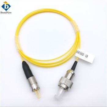
If you’re looking for a reliable laser chip partner, whether for a high-volume consumer product, a medical device, an industrial system, or a space application, our team can work with you to customize a solution that fits your requirements and budget. We can provide sample units, compliance testing data, and flexible lead times to meet your timeline. Don’t hesitate to reach out to our sales team to discuss your project details and start collaborating on the right laser chip solution for your needs.
COS Laser Diode References
- International Data Corporation (IDC). Global Laser Diode Market Forecast, 2023–2027.
- U.S. Department of Energy. Advanced Manufacturing for Photonic Devices: Thermal Management Challenges. 2022.
- European Commission. Photonic Integrated Circuits for Medical Applications: Regulatory Roadmap. 2023.
- Optoelectronics Industry Development Association (OIDA). VCSEL and Laser Chip Performance Metrics, 2024.
Hangzhou Brandnew Technology Co., Ltd.
Hangzhou Brandnew Technology Co., Ltd. is one of the leading laser chip manufacturers and suppliers in China, has a professional factory which manufacturers high quality laser chip and sells at competitive price. Welcome to wholesale our products made in China.
Address: 17F,Building 2, Aoqiang Mansion, No. 6 Xiyuan 5th Rd,310030 Hangzhou,China
E-mail: admin@brandnew-china.com
WebSite: https://www.brandnewdiode.com/
